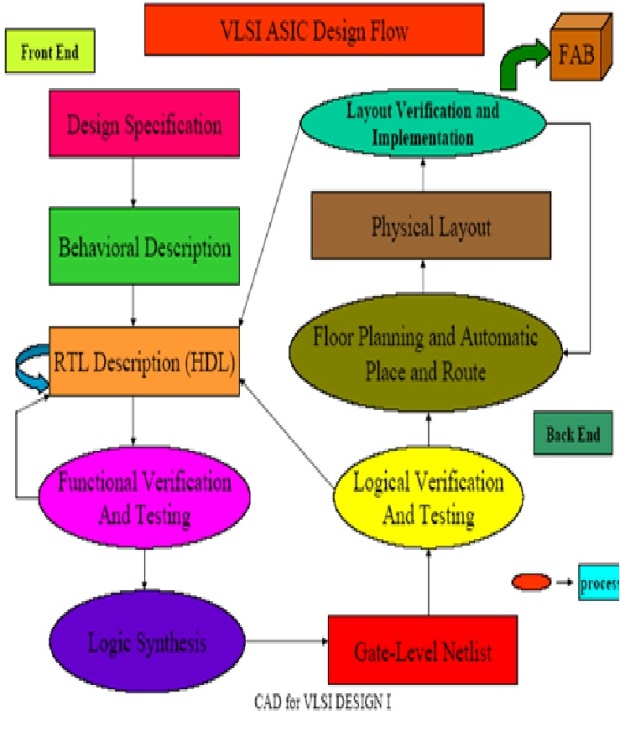
Continuing from the previous post about ASIC Design Flow Part-1, here is some detail explanation about backend flows.
Backend flow
In a typical ASIC back-end flow, the main steps in the ASIC physical design flow are:
- Design Netlist (after synthesis)
- Floorplanning
- Partitioning
- Placement
- Clock-tree Synthesis (CTS)
- Routing
- Physical Verification
- GDS II Generation
These steps are just the basic. There are detailed PD flows that are used depending on the Tools used and the methodology/technology. Some of the tools/software used in the back-end design are :
- Cadence (SOC Encounter, VoltageStorm, NanoRoute)
- Synopsys (Design Compiler, IC Compiler)
- Magma (BlastFusion, etc.)
- Mentor Graphics (Olympus SoC, IC-Station, Calibre)
Backend tools
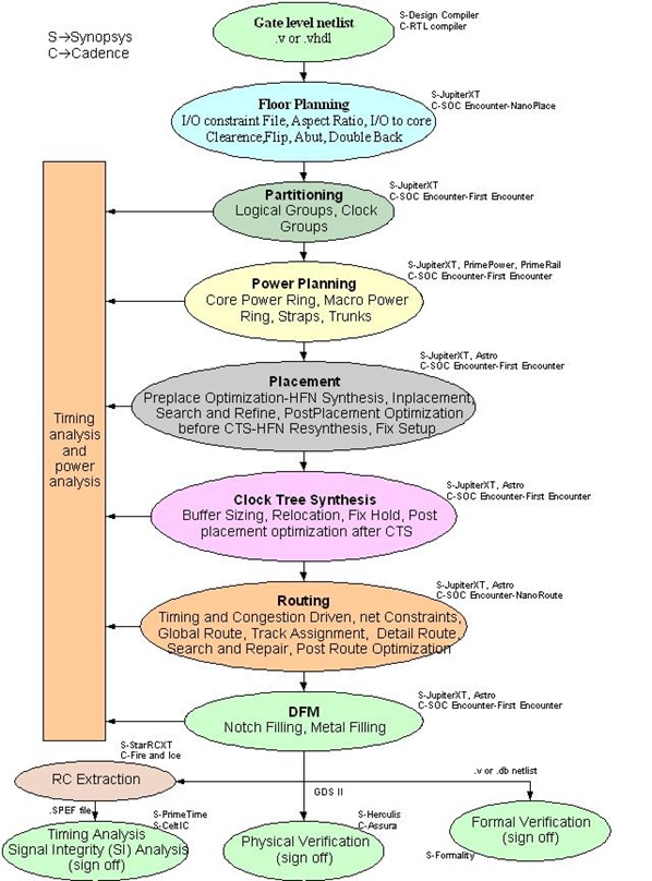
A more detailed Physical Design Flow is shown below. Here you can see the exact steps and the tools used in each step outlined.
The ASIC physical design flow uses the technology libraries that are provided by the fabrication houses. Technologies are commonly classified according to minimal feature size. Standard sizes, in the order of miniaturization, are 2μm, 1μm , 0.5μm , 0.35μm, 0.25μm, 180nm, 130nm, 90nm, 65nm, 45nm, 28nm, 22nm, 18nm, 14nm, etc. They may be also classified according to major manufacturing approaches: n-Well process, twin-well process, SOI process, etc.
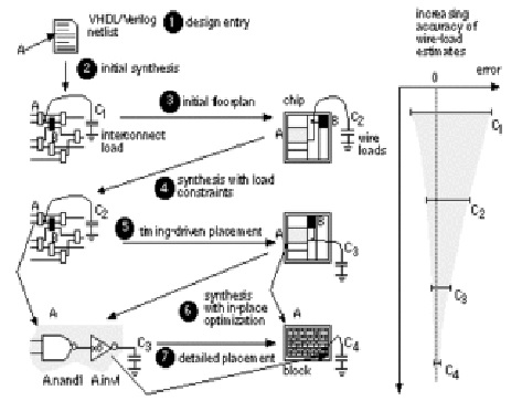
1.) Design Netlist
Physical design is based on a netlist which is the end result of the Synthesis process. Synthesis converts the RTL design usually coded in VHDL or Verilog HDL to gate-level descriptions which the next set of tools can read/understand. This netlist contains information on the cells used, their interconnections, area used, and other details. Typical synthesis tools are:
- Cadence RTL Compiler/Build Gates/Physically Knowledgeable Synthesis (PKS)
- Synopsys Design Compiler
During the synthesis process, constraints are applied to ensure that the design meets the required functionality and speed (specifications). Only after the netlist is verified for functionality and timing it is sent for the physical design flow.
Physical Design Steps:
2.) Floorplanning
The first step in the physical design flow is Floorplanning. Floorplanning is the process of identifying structures that should be placed close together, and allocating space for them in such a manner as to meet the sometimes conflicting goals of available space (cost of the chip), required performance, and the desire to have everything close to everything else.
Based on the area of the design and the hierarchy, a suitable floorplan is decided upon. Floorplanning takes into account the macros used in the design, memory, other IP cores and their placement needs, the routing possibilities and also the area of the entire design. Floorplanning also decides the IO structure, aspect ratio of the design. A bad floorplan will lead to waste-age of die area and routing congestion.
In many design methodologies, Area and Speed are considered to be things that should be traded off against each other. The reason this is so is probably because there are limited routing resources, and the more routing resources that are used, the slower the design will operate. Optimizing for minimum area allows the design to use fewer resources, but also allows the sections of the design to be closer together. This leads to shorter interconnect distances, less routing resources to be used, faster end-to-end signal paths, and even faster and more consistent place and route times. Done correctly, there are no negatives to floorplanning.
As a general rule, data-path sections benefit most from floorplanning, and random logic, state machines, and other non-structured logic can safely be left to the placer section of the place and route software.
Data paths are typically the areas of your design where multiple bits are processed in parallel with each bit being modified the same way with maybe some influence from adjacent bits. Example structures that make up data paths are Adders, Subtractors, Counters, Registers, and Muxes.
3.) Partitioning
Partitioning is a process of dividing the chip into small blocks. This is done mainly to separate different functional blocks and also to make placement and routing easier. Partitioning can be done in the RTL design phase when the design engineer partitions the entire design into sub-blocks and then proceeds to design each module. These modules are linked together in the main module called the TOP LEVEL module. This kind of partitioning is commonly referred to as Logical Partitioning.
4.) Placement
Before the start of placement optimization all Wire Load Models (WLM) are removed. Placement uses RC values from Virtual Route (VR) to calculate timing. VR is the shortest Manhattan distance between two pins. VR RCs are more accurate than WLM RCs.
Placement is performed in four optimization phases:
- Pre-placement optimization
- In placement optimization
- Post Placement Optimization (PPO) before clock tree synthesis (CTS)
- PPO after CTS.
- Pre-placement Optimization optimizes the netlist before placement, HFNs are collapsed. It can also downsize the cells.
- In-placement optimization re-optimizes the logic based on VR. This can perform cell sizing, cell moving, cell bypassing, net splitting, gate duplication, buffer insertion, area recovery. Optimization performs iteration of setup fixing, incremental timing and congestion driven placement.
- Post placement optimization before CTS performs netlist optimization with ideal clocks. It can fix setup, hold, max trans/cap violations. It can do placement optimization based on global routing. It re does HFN synthesis.
- Post placement optimization after CTS optimizes timing with propagated clock. It tries to preserve clock skew.
5.) Clock tree synthesis
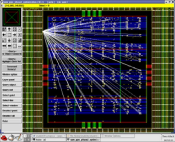
Backend: CTS tool
Ideal clock before CTS:
The goal of clock tree synthesis (CTS) is to minimize skew and insertion delay. Clock is not propagated before CTS as shown in the picture. After CTS hold slack should improve. Clock tree begins at .sdc defined clock source and ends at stop pins of flop. There are two types of stop pins known as ignore pins and sync pins. ‘Don’t touch’ circuits and pins in front end (logic synthesis) are treated as ‘ignore’ circuits or pins at back end (physical synthesis). ‘Ignore’ pins are ignored for timing analysis. If clock is divided then separate skew analysis is necessary.
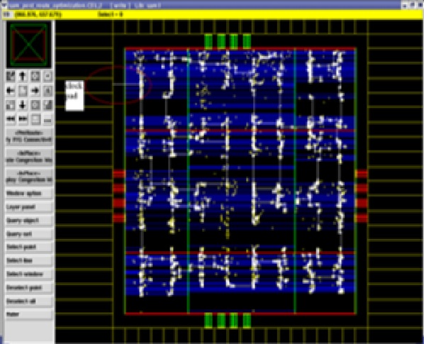
Backend: CTS tool output
- Global skew achieves zero skew between two synchronous pins without considering logic relationship.
- Local skew achieves zero skew between two synchronous pins while considering logic relationship.
- If clock is skewed intentionally to improve setup slack then it is known as useful skew.
Rigidity is the term coined in Astro to indicate the relaxation of constraints. Higher the rigidity tighter is the constraints.
Clock After CTS
In clock tree optimization (CTO) clock can be shielded so that noise is not coupled to other signals. But shielding increases area by 12 to 15%. Since the clock signal is global in nature the same metal layer used for power routing is used for clock also. CTO is achieved by buffer sizing, gate sizing, buffer relocation, level adjustment and HFN synthesis. We try to improve setup slack in pre-placement, in placement and post placement optimization before CTS stages while neglecting hold slack. In post placement optimization after CTS hold slack is improved. As a result of CTS lot of buffers are added. Generally for 100k gates around 650 buffers are added.
6.) Routing
There are two types of routing in the physical design process, global routing and detailed routing. Global routing allocates routing resources that are used for connections. Detailed routing assigns routes to specific metal layers and routing tracks within the global routing resources.
7.) Physical Verification
Physical verification checks the correctness of the generated layout design. This includes verifying that the layout
- Complies with all technology requirements – Design Rule Checking (DRC)
- Is consistent with the original netlist – Layout vs. Schematic (LVS)
- Has no antenna effects – Antenna Rule Checking
- Complies with all electrical requirements – Electrical Rule Checking (ERC).
Physical Verification flow
8.) GDS II (Calma GDS II)
GDS = Graphic Database System
Initially, GDSII was designed as a format used to control integrated circuit photomask plotting. Despite its limited set of features and low data density, it became the industry conventional format for transfer of IC layout data between design tools of different vendors, all of which operated with proprietary data formats
GDS II is a database file format which is the de facto industry standard for data exchange of integrated circuit or IC layout artwork. It is a binary file format representing planar geometric shapes, text labels, and other information about the layout in hierarchical form. The data can be used to reconstruct all or part of the artwork to be used in sharing layouts, transferring artwork between different tools, or creating photo masks. Initially, GDS II was designed as a format used to control integrated circuit photo mask plotting. Despite its limited set of features and low data density, it became the industry’s default format for transfer of IC layout data between design tools of different vendors, all of which (at that time) operated with often incompatible and proprietary data formats. It was originally developed by Calma for its layout design software, “Graphic Data System” (“GDS”) and “GDS II”. Now the format is owned by Cadence Design Systems. GDS II files are usually the final output product of the IC design cycle and are given to IC foundries for IC fabrication. GDS II files were originally placed on magnetic tapes. This moment was fittingly called tape out though it is not the original root of the term. Objects contained in a GDS II file are grouped by assigning numeric attributes to them including “layer number”, “datatype” or “texttype”. While these attributes were designed to correspond to the “layers of material” used in manufacturing an integrated circuit, their meaning rapidly became more abstract to reflect the way that the physical layout is designed. As of October 2004, many EDA software vendors have begun to support a new format, OASIS, which may replace GDS II.
Hope that this clears basic idea about backend processes happening during various stages.

[…] have got a high level idea about overall ASIC design flow. I will discuss the Backend flow in my upcoming post (ASIC Design Flow outline Part-2) […]
LikeLiked by 1 person
Tks for sharing your knowledge! I’m not a technical person starting managing microeletronics projects, and this information was very important to clarify a lot of aspects of this proccess. I’ll keep learning. Regards
LikeLike