Today, ASIC design flow is a very sophisticated and developed process. The overall ASIC design flow and the various steps within the ASIC design flow have proven to be both practical and robust in multi-millions ASIC designs until now. Let’s discuss about an overview of these steps in the design flow.
1) SPECIFICATION:
Lot of activity from gathering market requirement to deciding the technical aspect is done first. This is the crucial step as it will affect the future of the product. Here, vendors may want to get feedback from potential customers on what they are looking for. Once this is done final specification sheet with all possible technical details is made and handed over to the next team.
2) ARCHITECTURE:
This is where the main work starts. With the help of the specification sheet the target IC’s architecture is decided and a layout for same is created by design engineers using EDA tools. In the next step this architecture is implemented and tested with the help of programming language and tools.
Flowcharts for Design Flow:
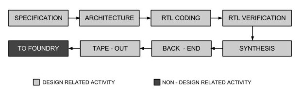
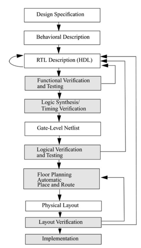
VLSI Design Flow
ASIC Design Flow (Courtesy: Verilog HDL by Samir Palnitkar)
3) RTL CODING:
RTL is an acronym for register transfer level. This implies that the VHDL code written based on the architecture describes how data is transformed as it is passed from register to register. This is how a 2-input MUX looks like :
module mux_2x1(input A, input B, input sel, output Y);

assign Y = (sel) ? (A) : (B);

endmodule
4) RTL VERIFICATION:
Register Transfer Level (RTL) simulation and verification is one of the important step. This ensures that the design is logically correct and without major timing errors. It is advantageous to perform this step, especially in the early stages of the design. Synopsys simulation tools may be used to perform RTL verification. A test bench file may be used here for verification.
5) SYNTHESIS:
This is where the design now start to get physical. Logic synthesis is a process by which the desired circuit behavior i.e. Register Transistor Level is turned into a design in terms of logic gates which drives the circuit or architecture. This is done with the help of FPGA/CPLD/ASIC hardware tools. These target boards may be accessed using the IDE’s provided by specific vendor.
Logic synthesis tools convert the RTL design description to a gate-level “netlist” or a “list of wires”. A gate-level netlist is a description of entire chip in terms of logic gates and their interconnections. Synthesis tools ensure that the gate-level netlist meets timing, area, and power specifications.
6) BACKEND:
Here the final tested design after synthesis is given to the IC manufacturer. The gate-level netlist is input to an Automatic Place and Route tool, which creates a layout. The layout is verified and then fabricated on a chip. Here, the gate level netlist is converted to a complete physical geometric representation.
7) TAPEOUT:
Tape out is the process under backend only where the final result of FRONTEND (first 5 steps) is provided to the manufacturer in form of photomask. Then the manufacturer performs wafer processing, packaging, testing, delivery of samples to test the physical IC. The file produced at the output of the layout is the GDSII (GDS2) file which is the file used by the foundry to fabricate the silicon. The layout should be done according the silicon foundry design rules.
8) FOUNDRY:
Once the sample are tested and all the requirement are furnished the design is sent for mass production.
To summarize the above steps, following are the main points to be noted:
- Specifications comes first, they describe abstractly the functionality, interface, and the architecture of the digital IC circuit to be designed.
- Behavioral description is then created to analyze the design in terms of functionality, performance, compliance to given standards, and other specifications.
- RTL description is done using HDLs. This RTL description is simulated to test functionality. From here onwards we need the help of EDA tools.
- RTL description is then converted to a gate-level netlist using logic synthesis tools. A gate-level netlist is a description of the circuit in terms of gates and connections between them, which are made in such a way that they meet the timing, power and area specifications.
- Finally a physical layout is made, which will be verified and then sent to fabrication.
As of today’s world, most of the digital design activity is concentrated on manually optimizing the RTL description of the circuit. The frontend is the only manual step in entire flow. After the RTL description is frozen, lots of EDA tools from different vendors are available to assist the designer in further processes.
Hope that you have got a high level idea about overall ASIC design flow. I will discuss the Backend flow in my upcoming post (ASIC Design Flow outline Part-2) …

[…] from the previous post about ASIC Design Flow Part-1, this post on it’s […]
LikeLiked by 1 person
Hi Sharvill,
Can you please explain deep on uvm topology (hierarchy) from the log file and what does it signifies?
Thanks
LikeLiked by 1 person
Sure.. I will create a post for the same. Thanks for the feedback!
LikeLiked by 2 people
#freevlsitutorial To help you with Self learning is the motto of our YouTube channel. Lets learn about ASIC Design Flow with step by step explanation given by Mr. P R Sivakumar- CEO, Maven Silicon.
https://www.youtube.com/channel/UCu19H6thv_ad_Sl2cG-t-jA
LikeLike
Thanks Madhura for sharing the pointers!
LikeLike
#freevlsitutorial To help you with Self learning is the motto of our YouTube channel. Lets learn about ASIC Design Flow this week with step by step explanation given by Mr. P R Sivakumar- CEO, Maven Silicon.
LikeLike
[…] ASIC Design Flow Block Diagrams […]
LikeLike
The VLSI design course online will last 15-20 weeks and will provide both theoretical and practical learning under the supervision of fantastic and experienced faculty members. Netlist, GDSII, Power Planning, Floor Planning, Global Routing, and TCL Scripting are some of the concepts you’ll master. Apart from these, you will also learn about other subjects from industry experts, and you will be fascinated by working on real-world manufacturing projects once you have completed the course. Contact Us: 9483440125
LikeLike
It sets some fundamental rules for measuring profits, controlling expense, and building a growing bankroll. The reality is that poker mastery requires a fantastic deal of skill. This may set the other gamers on alert.
LikeLike